
Samsung Unveils Nano City in Pyeongtaek for Advanced Chip Production
Samsung Electronics has announced the launch of its new Nano City in Pyeongtaek, South Korea. The facility is positioned as a key hub for advanced semiconductor production and technological innovation.
 Radwan AbdulhadiEditor and technology writer
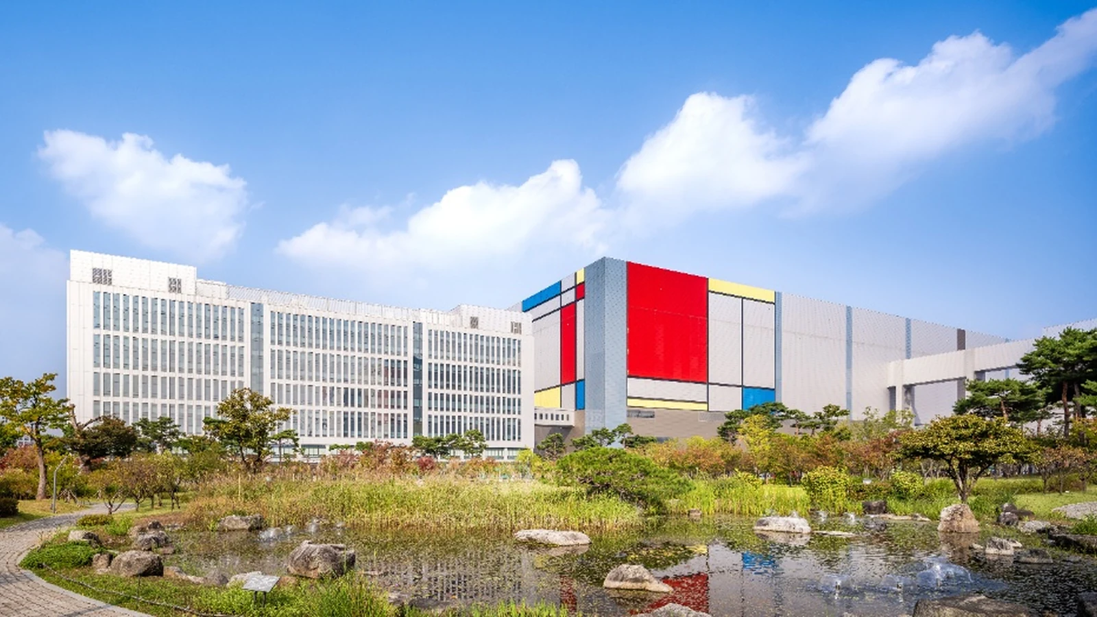
Introduction to the Pyeongtaek Facility
Samsung Electronics has officially introduced its new Nano City in Pyeongtaek, a significant addition to its global semiconductor footprint. This announcement marks a strategic move by the company to consolidate and expand its production capabilities in one of South Korea's key industrial regions. The facility is designed to support the next generation of semiconductor technologies, reflecting the company's ongoing commitment to maintaining its position as a leader in the global chip market. By establishing this new hub, Samsung aims to streamline its manufacturing processes and improve efficiency in producing advanced components that are essential for modern electronic devices. Further details are available from Samsung Global Newsroom in the original source material.
Strategic Importance of the Location
The selection of Pyeongtaek as the site for the new Nano City underscores the region's established role in the semiconductor industry. Pyeongtaek is already home to several major semiconductor facilities, creating a robust ecosystem of suppliers, talent, and infrastructure that supports high-tech manufacturing. By locating the new Nano City in this area, Samsung can leverage existing logistical networks and skilled labor pools, which are critical for the complex and precise nature of chip fabrication. This geographic concentration allows for better coordination between different stages of the production process, potentially reducing lead times and enhancing overall operational resilience. The move also aligns with national efforts to strengthen South Korea's position as a global leader in semiconductor technology. Further details are available from campus images in the original source material.
Focus on Advanced Manufacturing
While specific technical specifications for the new facility have not been detailed in the initial announcement, the term "Nano City" suggests a focus on nanoscale manufacturing processes. These processes are fundamental to producing the high-performance chips used in smartphones, data centers, and artificial intelligence systems. Samsung has long been at the forefront of developing smaller and more efficient transistors, and this new facility is expected to play a crucial role in that ongoing evolution. The company's investment in such advanced infrastructure indicates a long-term strategy to meet the growing demand for powerful computing capabilities. As devices become more complex, the need for precise and reliable manufacturing becomes even more critical, making facilities like the Pyeongtaek Nano City indispensable.
Corporate Communication and Media Engagement
The announcement was disseminated through the Samsung Global Newsroom, which serves as the central hub for the company's official communications. This platform provides journalists, investors, and the public with accurate and timely information about Samsung's latest developments. By using this channel, Samsung ensures that its message is consistent and authoritative across different regions and media outlets. The newsroom also offers resources for media inquiries, allowing reporters to seek further clarification or additional details about the new facility. This structured approach to communication helps maintain transparency and builds trust with stakeholders who are interested in the company's strategic initiatives and technological advancements.
Broader Industry Implications
The establishment of the Nano City in Pyeongtaek has broader implications for the global semiconductor industry. As competition intensifies among major chipmakers, the ability to scale production and maintain technological leadership is paramount. Samsung's move reinforces its commitment to staying at the cutting edge of semiconductor technology, which is a cornerstone of the modern digital economy. The facility is expected to contribute to the supply chain for various high-tech products, ensuring that Samsung can meet the demands of its diverse customer base. Furthermore, the investment in new infrastructure signals confidence in the long-term growth of the semiconductor sector, despite the challenges posed by geopolitical tensions and supply chain disruptions.
Customer and Stakeholder Support
While the primary focus of the announcement is on the industrial and technological aspects of the new facility, Samsung also emphasizes its commitment to supporting its customers and stakeholders. For any issues related to customer service, the company directs users to its dedicated support channels, ensuring that assistance is readily available. This approach reflects Samsung's broader corporate philosophy of integrating operational excellence with strong customer relations. By providing clear pathways for support and media inquiries, Samsung aims to foster a positive and informed relationship with all parties involved in its business operations. This holistic strategy is crucial for maintaining brand loyalty and trust in an increasingly competitive market.
Sources
- Samsung Global NewsroomSamsung Nano City – Pyeongtaek